
Additive vs. Subtractive Manufacturing of Thin Film Micro Circuits
Sputtering and photolithography vs. chemical etching—the advantages are clear.
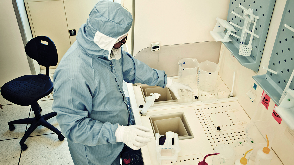
Device makers have a choice of whether to specify an additive or subtractive process for fabricating the micron-scale circuits used in their products. Knowing the basic differences between the two is important. Medical sensor device and RF component engineers and designers have a choice of whether to specify an additive or subtractive process for fabricating the ultra-miniature or micron-scale micro circuits that are best for their products. Knowing the basic differences between the two thin film technologies is important, because the change in the micro circuit's electrical performance and the lot yield per run can be significant.
In general, an additive process to micro circuits is much more likely to achieve:
- Higher circuit resolution (more conductive traces packed into a smaller area)
- More consistent trace definition
- Thinner and therefore more flexible circuits (where needed)
- More uniform circuit lines (i.e., same width top and bottom)
- More consistent circuit electrical and mechanical performance
- More control across a wider range of circuit resolution, flexibility/rigidness, and trace thickness
Additive Versus Subtractive — the Basics
In order to understand why these advantages exist, it helps to have a basic understanding of how the two technologies work. Both methods are used to create circuit lines on a surface. Like its name implies, a subtractive technology creates circuit lines by subtracting or removing material — in this case, metal from a surface pre-bonded to a non-metallic polyimide base. The metallic material is removed using chemical etching, so what’s left are the circuit lines with spaces between them.
An additive process creates circuit lines by sputtering a positively charged metal to a negatively charged base, then, if needed, plating to build up conductive traces of precise height and width. The base may be either a conductive material or non-conductive polyimide to which a metallic layer was applied. Using photolithography, a photoresist “stencil” is applied on top of this conductive layer. The plated metal is attracted and bonds with the conductive layer where the nonconductive photoresist has left it exposed.
In both types of process, what manufacturers use as their base is the one key in how well the finished circuit will perform. If the base is an “off the shelf” product (e.g., a metal-bonded-to-polyimide stock), these stocks only come in certain thicknesses, which obviously limits circuit size and flexibility. Rather than buy stock, an alternative approach is to spin coat the base layer — which, in Metrigraphics’ case, can be as thin as 4 microns. (When we say we have a “proprietary” additive process, part of what makes it proprietary is our unique ability to sputter a very thin metallic base layer.)
An additive process may also employ laminate stocks, an approach that again limits the ability to control thickness and flexibility precisely. Another drawback of laminates is how they are used to create circuits with multiple layers — with an adhesive layer that bonds the laminate layers together. That adhesive layer is typically 50 microns thick, further limiting how small and flexible the circuit can be, as well as the ability to control size and flexibility in precise increments.
Additive’s Secret Sauce
A large part of what gives additive processing all the advantages listed above is photolithography, which is inherently more precise than chemical etching your medical sensor or RF micro circuits. Lines will be more precisely defined and will be the same width at the top and at the base, versus what is typically achieved with etching (lines thicker at the base.) Greater resolution and line uniformity means greater component reliability, especially at a much smaller scale.
So, why doesn't every micro circuit manufacturer make circuits this way?
While additive is necessary for achieving these results, it is not sufficient. Additive processing at this scale means you can’t just design the product; you also have to design the process that makes the product. One of additive’s virtues is that any two batches of the same product should be virtually identical. However, because of the technology involved, the way two different products are produced could be significantly different. Tailoring an additive process calls for considerable knowledge and experience with this technology. And that’s something else equipment makers should consider when specifying how their ultra-miniature rigid and flexible circuits get made.
Contact us today for more information about our circuit manufacturing capabilities.
1001 Pawtucket Blvd,
Lowell, MA 01854
Privacy Policy