
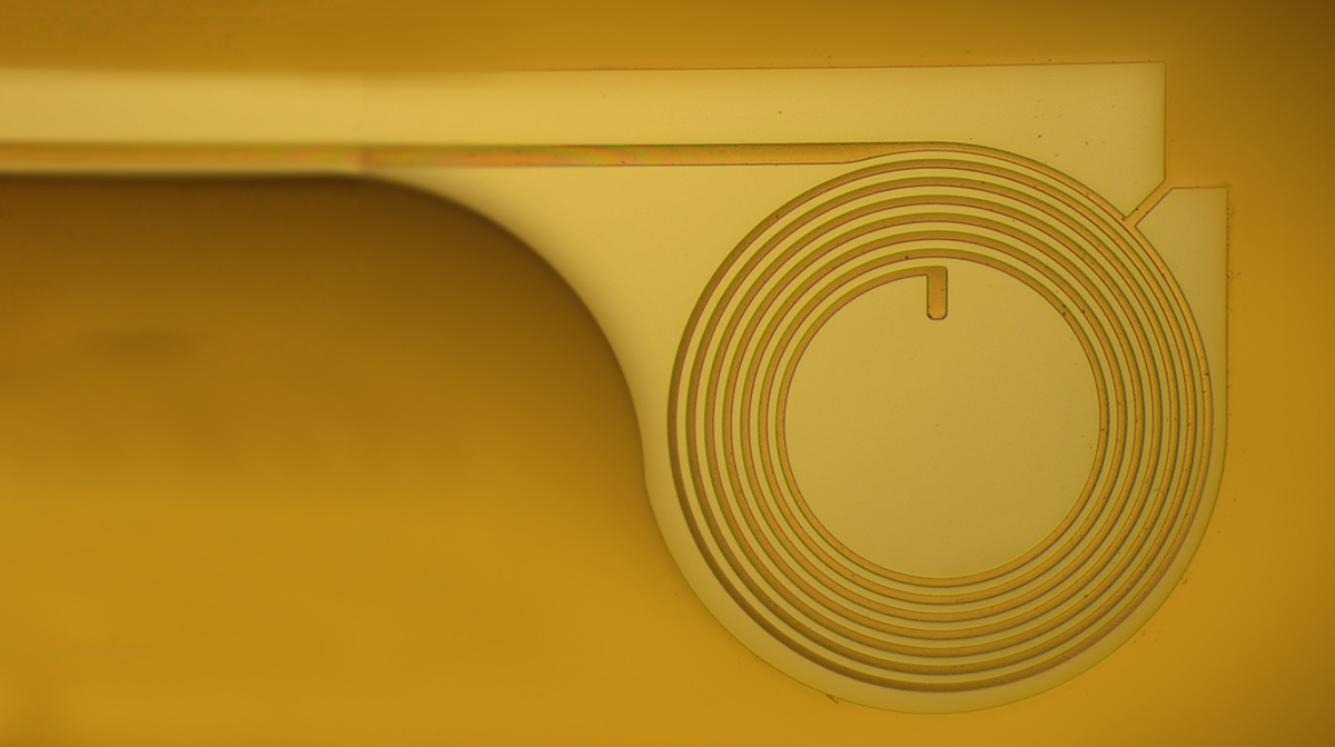
New Advanced Microcircuit Metallization Process
We have developed an advanced process for applying metal layers to circuit substrates and to polyimide layers on multilayer circuits. The process works for both rigid and flexible circuits.
The new process achieves superior results based on a number of important market criteria, including a wide range of component sizes, coating thicknesses, substrate materials, and coating materials. And it has excellent adhesion properties.
Technologies involved can include sputtering, electroplating, and thermal evaporation depending on such factors as the type and size of substrate and the metal to be applied.
Metalization layers can range in thickness from 10 microns to over 100 microns. Substrates can range up to 12” X 12” or 144 square inches. Chrome and Inconel can be deposited on substrates up to 85” long using a dual-chamber thermal evaporator.
The range of suitable substrates includes glass, metals and polymer films, among others.
Product manufacturers interested in learning whether our advanced metallization process is suitable for their application should contact us.
1001 Pawtucket Blvd,
Lowell, MA 01854
Privacy Policy