
Providing Our Customers with Reliable Photolithography Resolution
Are you looking for a reliable photolithography partner? Our proprietary photolithography process ensures that you get more consistent trace definition, thinner and therefore more flexible circuits (where needed) AND more uniform circuit lines (i.e., same width top and bottom).
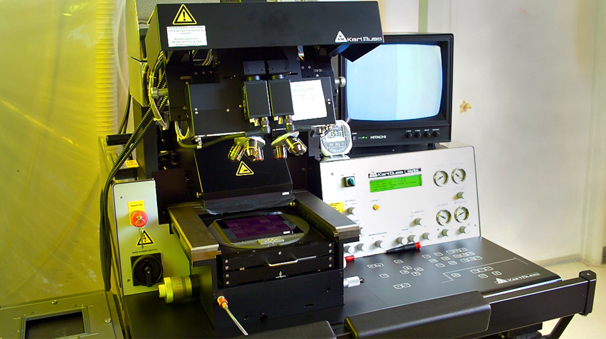
Our process defines patterns at extremely fine resolutions on substrates that range in size from very small to very large, using a broad range of liquid and dry photo-resist films. It creates circuit lines by sputtering a positively charged metal to a negatively charged base, then, if needed, plating to build up conductive traces of precise height and width. This allows us to get precision that our competitors can't.
Our photolithography process achieves image resolutions of one to two microns on substrates up to 12" x 12". The benefits to you? You get higher circuit resolution (more conductive traces packed into a smaller area) and more consistent circuit electrical and mechanical performance. And we can do this consistently, from prototype to high-volume production.
Contact our team to learn more about how we can help you on your next photolithography project.
1001 Pawtucket Blvd,
Lowell, MA 01854
Privacy Policy