
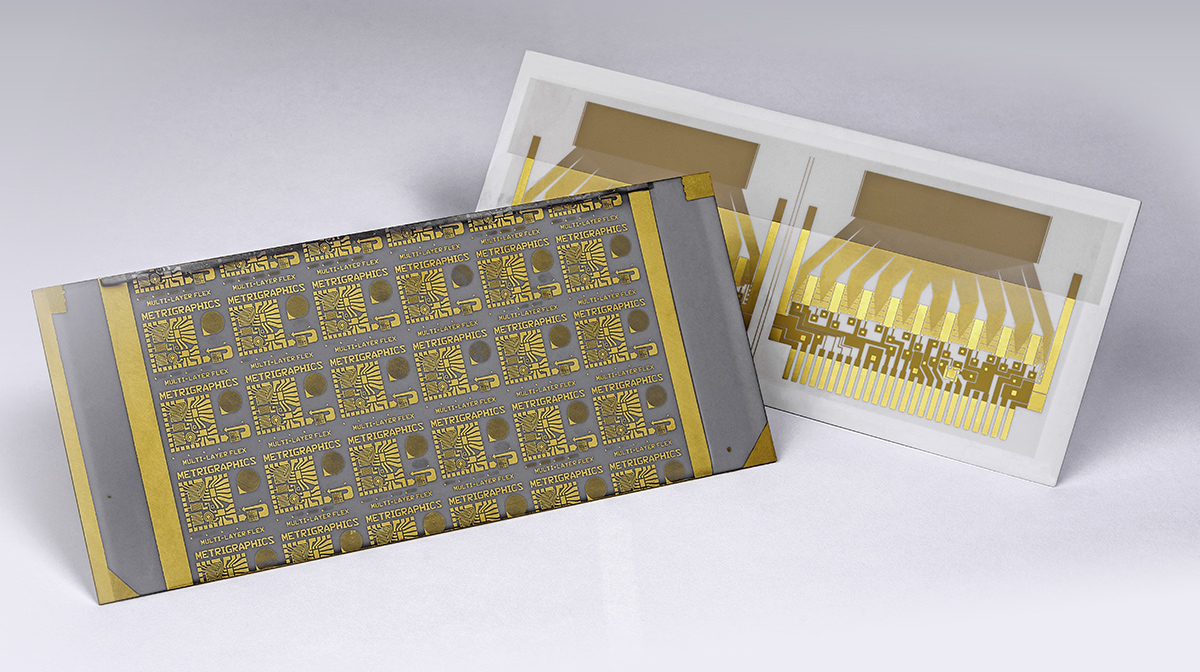
Additive Advantages of Thin Film Manufacturing: Less Time, Less Metal, Less Money
In an earlier blog post we discussed why micron-scale circuits tend to perform better when made using an additive versus a subtractive process. The additive process defines circuit lines by adding (electroplating) conductive material on top of a thin metal film that’s been sputtered onto a substrate. The subtractive process defines circuit lines by removing (chemical etching) conductive material out of a thick metal film that’s been sputtered onto a substrate. The places where metal is either added or subtracted are defined by a stencil of photoresist material that remains on the metal film following photolithography.
Performance disadvantages from thin film's subtractive process come from the fact that the chemical etching agents have more time to work at the top of the channel being carved out between circuit lines than at the bottom. This results in circuit lines that tend to be wider (and the spaces between them narrower) at the bottom than at the top. This difference is particularly relevant in miniature components where a few microns of variation is a greater percentage of line width in circuits with very narrow traces than in circuits with wider traces.
As we noted before, what this variation means in terms of circuit performance is that the additive process will likely achieve:
- More uniform circuit lines (i.e., same width top and bottom)
- More consistent trace definition
- More consistent circuit electrical and mechanical performance
- Thinner and therefore more flexible circuits (where needed)
- Higher density circuit resolution (more conductive traces packed into a smaller area)
- More control across a wider range of circuit resolution, flexibility/rigidness, and trace thickness
Beyond the Circuit’s Own Advantages
All the advantages listed above relate to the physical and electrical characteristics of the device itself. But thin film circuits manufactured with an additive process aren’t just better circuits, they also take less time and use less precious metal (and therefore money) to manufacture. Considering that the metal is often gold, it’s easy to see why less metal used means less expense.
Additive’s manufacturing advantage comes from the fact that the process adds metal by electroplating. In electroplating virtually all the plating metal electrically bonds to a thin layer of metal pre-deposited on the substrate. This results in a very efficient utilization of the precious metals with none being thrown away as waste or reclaimed later as is required with a subtractive process.
With the subtractive process, more metal than is required is sputtered onto the substrate prior to circuit line definition so there will be more metal available later to be etched away to form channels. Sputtering is a process that uses a plasma to eject material from a metal target and deposit it onto a substrate. However, unlike electroplating, not all the metal ends up on the substrate. Some of it deposits on the walls of the reaction chamber and must be removed or reclaimed — adding extra time and expense. Another reason that sputtering adds time and expense is that it is less efficient than electroplating at bonding metal to metal, so it takes longer to do it.
Are you considering a miniature circuit for your next design? Ask us for a quote.
1001 Pawtucket Blvd,
Lowell, MA 01854
Privacy Policy